How to Create a Clear and Effective PCB Schematic
A well organised schematic is really important for good PCB design. It helps make the layout phase easier and makes fixing problems simpler. Here are some easy tips to help you create a clear schematic:
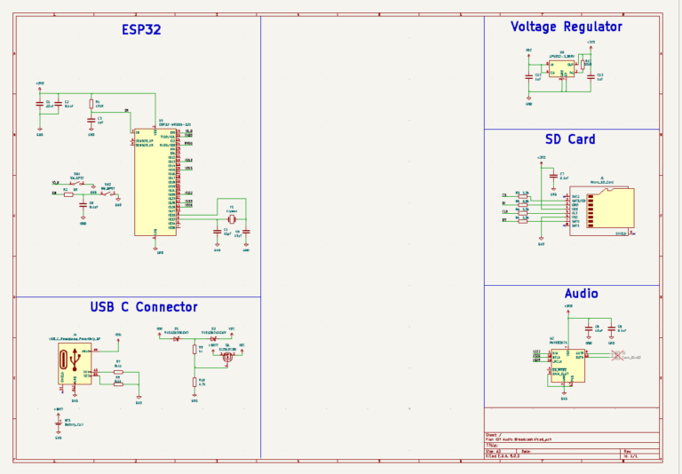
A well-organized schematic is really important for good PCB design. It helps make the layout phase easier and makes fixing problems simpler. Here are some easy tips to help you create a clear schematic:
- Use Common Symbols: Always use standard symbols for your components so that anyone looking at your design can easily understand it.
- Group Components Sensibly: Put components that work together near each other. For example, group power components in one area and signal components in another. This makes the design easier to follow.
- Label Everything Clearly: Give each part a unique name (like R1 for the first resistor, C1 for the first capacitor) and use simple names for connections, such as VCC for power or GND for ground.
- Keep Wires Neat and Straight: Draw straight lines and avoid crossing wires when you can. A clean, tidy schematic is easier to read and understand.
- Use Nets Instead of Wires: Instead of drawing long wires, use nets (labels) to show connections. This keeps your schematic neat and less confusing, especially when working with big designs.
- Use Hierarchical Design for Complex Circuits : For larger designs, break them into smaller blocks or sections. Each block can represent a part of the circuit. This helps keep the schematic organized.
- Add Notes: Write notes to explain any tricky or important parts of the design. This will help you or anyone else understand your work later on.
- Use Power Symbols: Instead of drawing wires for every power or ground connection, use symbols like VCC or GND to keep the schematic clean.
- Plan for Testing: Add test points where you can easily measure signals while testing your board. Make sure important parts of the circuit are easy to reach.
- Check for Errors: Always run a design check to catch any mistakes, like missing connections. Fixing these early saves trouble later on.
By following these tips, you can make a schematic that’s easy to read and ready for the next step in PCB design. A clear schematic saves time and helps avoid mistakes.
And if you need help with your project, feel free to reach out—I’m here to help.