The PCB Design Process: From Concept to Final Layout
Printed Circuit Boards (PCBs) are crucial for the electronics we use every day, from phones to computers. A good PCB design is key to making sure devices work well and last a long time.
Knowing the PCB design process is important for engineers, designers, and hobbyists. It helps create efficient designs and avoids mistakes that can cause problems later. In this post, I will break down the steps in the PCB design process, guiding you from your initial idea to a finished product.
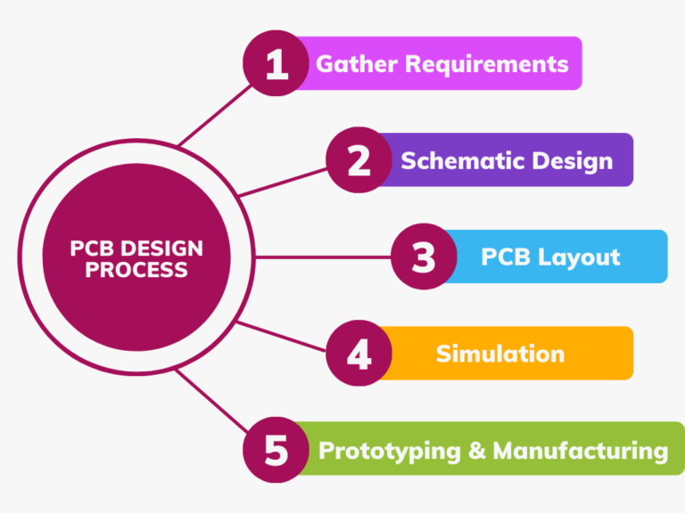
Step 1: Gathering Requirements
Before starting your PCB design, it’s important to gather all the details you need. This step is like planning a project before you jump in. Here’s what to consider:
- What’s the Purpose? :Figure out what you want your PCB to do. Is it for a gadget like a sensor, a power supply, or a Bluetooth device?
- Choose Your Components: List the parts you’ll need, such as chips, resistors, and connectors. Make sure they work well together.
- Power Needs: Decide how much power your PCB will need. Think about the voltage and current requirements.
- Size and Shape: Think about how big your PCB needs to be. It should fit in whatever device you’re building.
- Follow the Rules: Check if there are any rules or standards your PCB has to meet, like safety requirements.
By gathering this information first, you’ll set yourself up for a smoother design process and avoid problems later on.
Step 2: Schematic Design
Now that you have your requirements, it’s time to create the schematic. This is like a map showing how your PCB parts connect. Here’s how to do it:
- Choose Software: Pick a PCB design program you like, like Altium Designer, KiCad or Eagle.
- Add Parts: Place the components you listed in Step 1 onto the schematic, like ICs, resistors, capacitors, connectors etc.
- Connect Them: Draw lines (wires) to show how the components connect. Make sure it matches your plan and the datasheet of the ICs.
- Check for Errors: Use the software’s tools to find and fix mistakes, like missing connections.
- Label Everything: Clearly label each part and connection to make it easy to understand.
A clear schematic is key to a successful PCB design because it helps you in the next steps.
Step 3: PCB Layout
After creating your schematic, it’s time to turn it into a physical design with the PCB layout. This is where you decide how everything will fit on the board. Here’s how to do it:
- Set Up Your Board: Start by choosing the size and shape of your PCB based on your project requirements. Make sure it fits within your device.
- Place Components: Arrange the parts on the board according to your schematic. Think about where each part should go for the best performance.
- Route Traces: Connect the parts with traces (the lines on the board). Make sure to follow good practices, like keeping traces short and avoiding sharp turns.
- Check for Clearance: Ensure there’s enough space between traces and parts to avoid shorts. Check for any potential issues that might arise during manufacturing.
- Run Design Rules Check (DRC): Use the DRC tool in your software to find any design errors, like traces that are too close together. Fix any issues before moving on.
Creating a good PCB layout is essential for ensuring your design works well and can be manufactured successfully.
Step 4: Simulation
After completing your PCB layout, it’s time to test your design to ensure it works correctly. Here’s how to do it:
- Simulate the Circuit: Use simulation software to see how your circuit performs and catch potential issues on signal integrity, and thermal behaviour.
- Make Changes: If you find problems, adjust your design and fix any issues.
Step 5: Prototyping and Manufacturing
- After testing your PCB design, it’s time to make a prototype and get ready for production. Here’s how to do it:
- Make a Prototype: Send your design files to a manufacturer to create a prototype. This lets you see how your design works in real life.
- Assemble the Parts: Once you have the prototype, solder the components onto the board, making sure everything is in the right place.
- Test the Prototype: After putting it together, test the prototype to see if it works as expected. Check for any issues.
- Fix Any Problems: If you find issues during testing, make the necessary changes to your design. This could mean adjusting the layout or fixing connections.
- Get Ready for Production: When you’re happy with the prototype, prepare your final design for mass production. Make sure all the necessary files are ready for the manufacturer.
Making a prototype and testing it is important to ensure your PCB design works well before going into production.